You are here: Nature Science Photography – Image creation, Depth and Size – Photographic image creation
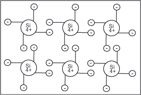
Digital recording technology thrives on the technical possibility of converting light into electricity by exploiting a photodiode’s junction photoelectric effect. Complicated term, isn’t it? But that’s not so bad! The technology is built around semiconductor components, which actually serve as the imaging source. The characteristics of semiconductors (silicon, germanium, selenium) fall between those of conductive metals (silver, copper, aluminium, gold) and non-conductive insulators (ceramics, glass, non-metals). Unlike metals, they conduct electricity better the warmer it is. The main component of most semiconductors is silicon, which has four electrons in its outer shell, the so-called valence electrons. Since silicon has a tendency to have eight valence electrons, it arranges itself in the form of a regular crystal lattice in which the four valence electrons of an atom combine with the corresponding electrons of a neighboring atom.

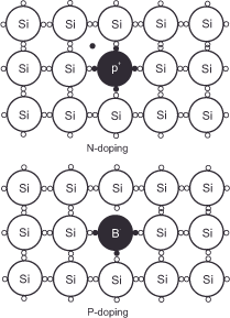
But in this form, the silicon crystal lattice is not yet electrically conductive. We deliberately contaminate the lattice with foreign atoms to achieve this, a process known as doping. We must use substances of different valence (with different numbers of valence electrons) to achieve conductivity, which requires a potential difference. In practice, these are phosphorus (valence level five, n-doping) and boron (valence level three, p-doping).

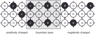
If the silicon crystal is n-doped, the phosphorus atom with its five valence electrons inserts itself into the lattice without any problems, but it only binds with the four neighboring silicon electrons, so that one of its valence electrons remains free. You’ve probably already guessed that with p-doping, the opposite situation arises. A boron atom has three valence electrons but needs four of them to form a stable electron pair bond with the neighboring silicon atoms. Therefore, a gap remains where an electron is absent. In practice, the impurities are few in number because there is one phosphorus or boron atom for every million silicon atoms. So much as a basis. For practical application, we dope one half of a silicon crystal with phosphorus and the other with boron, thus creating a p/n junction. The n-doped part is negatively charged due to excess electrons; the p-doped part has too few electrons (holes) and is positively charged. Since the atoms always strive to regularly fill their outer shells with four valence electrons, the excess electrons of the n-layer migrate into the holes of the p-layer, ensuring a low current flow. Since they move out of the center by the shortest route, a charge equilibrium develops there after a short time, which we call the junction. Once this has reached a certain width, the electrons can no longer make the jump to the other side, and the current flow collapses. The n-layer is now positively charged due to the released electrons; the p-layer is negatively charged due to the filled holes.

If we apply a voltage to the crystal lattice structured in this way from the outside, the following behavior results, depending on its polarity: If we apply the positive pole of the current source to the positively charged n-layer and the negative pole to the negatively charged p-layer, the excess electrons move from n through the current source to p. This widens the junction layer, preventing any more current from flowing through the silicon crystal. If we reverse the polarity, however, the positively charged n-layer receives plenty of electrons from the current source, so that there are even more excess electrons on this side. Simultaneously, the deprivation of electrons from the p-layer increases the number of holes on this side. In the end, the barrier layer dissolves and a current flows in the crystal lattice. The p-/n junction we made allows current to flow one way but blocks it the other. This behavior is called rectification, and the p-/n junction is called a diode.
For digital image acquisition, we make photodiodes whose n-layer facing the light is so thin that the light falls directly on the underlying barrier layer and can knock individual electrons out of it through its inherent energy. As more light strikes the barrier layer, it releases more electrons, which then migrate into the positively charged n-layer. The average ratio is one electron to every two photons. If we connect the n-layer and the p-layer via an electric circuit, the electrons flow across it from the n-layer to the p-layer, and light has become electric current. With an attached meter, we can easily measure the flow of light in this way, and we also make use of this with the light meter. To create an image, however, we still have to integrate the current flow over a certain time. An attached capacitor realizes this integration, and the entire process operates as follows: Before the exposure, we apply a voltage to the photodiode in the blocking direction to allow the capacitor to charge. In the course of the exposure, the capacitor is discharged according to the working principle of the photodiode, which is proportional to the amount of incident light. The resulting current flow is then digitized in the downstream analog/digital converter. – So, even a digital camera works internally with analog data first! Organized in large numbers into regular rows and columns, these photodiodes represent the sensor cells of the digital image carriers, known as photosites. They are, as a rule, square. The square photosites have side lengths ranging from 2 to 4 m for digital viewfinder cameras and 6 to 9 m for digital SLR cameras. This results in areas between 4-16 µm2 and 36-81 µm2. These size ratios become important when dealing with the contrast capability of the sensors, as the chapter about contrast does explain. Basically, we distinguish the digital recording media according to CCD sensors (charge-coupled devices) and CMOS elements (complementary metal oxide semiconductors).
Next Electronic image carriers – CCD and CMOS
Main Image creation, Depth and Size
Previous The reversal film
If you found this post useful and want to support the continuation of my writing without intrusive advertising, please consider supporting. Your assistance goes towards helping make the content on this website even better. If you’d like to make a one-time ‘tip’ and buy me a coffee, I have a Ko-Fi page. Your support means a lot. Thank you!


 Since I started my first website in the year 2000, I’ve written and published ten books in the German language about photographing the amazing natural wonders of the American West, the details of our visual perception and its photography-related counterparts, and tried to shed some light on the immaterial concepts of quantum and chaos. Now all this material becomes freely accessible on this dedicated English website. I hope many of you find answers and inspiration there. My books are on